Apple M3 Ultra Chip Could be a Monolithic Design Without UltraFusion Interconnect

erek

[H]F Junkie
Joined
Dec 19, 2005
Messages
10,923
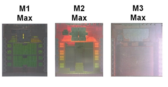
“While the absence of visible interconnect space on early die-shots is not conclusive evidence, as seen with the M1 Max not having visible UltraFusion interconnect and still being a part of M1 Ultra with UltraFusion, industry has led the speculation that the M3 Ultra may indeed feature a monolithic design. Considering that the M3 Max has 92 billion transistors and is estimated to have a die size between 600 and 700 mm², going Ultra with these chips may be pushing the manufacturing limit. Considering the maximum die size limit of 848 mm² for the TSMC N3B process used by Apple, there may not be sufficient space for a dual-chip M3 Ultra design. The potential shift to a monolithic design for the M3 Ultra raises questions about how Apple will scale the chip's performance without the UltraFusion interconnect. Competing solutions, such as NVIDIA's Blackwell GPU, use a high-bandwidth C2C interface to connect two 104 billion transistor chips, achieving a bandwidth of 10 TB/s. In comparison, the M2 Ultra's UltraFusion interconnect provided a bandwidth of 2.5 TB/s.”
1712067823570.png

Source: https://www.techpowerup.com/321129/...ithic-design-without-ultrafusion-interconnect
 
Well, I'm no apple fan boi (except for when those massive dividend checks arrive :D), but if anyone has the drive, resources, and engineering talent to make something that seems nearly impossible into something that works really well (like this no-interconnect thing) it's them fruity bois....

Yea it won't be cheap & it may take a little while, but as the saying goes "no pain, no gain" :D
Apple had the drive and resources to make their own CPU back in the day, and it was a huge financial failure. It was known as project aquarius. In the end they ended up going with Motorola 88K. Just a reminder that Apple is not at the same level of chip manufacturing as AMD and Intel. The M-series chips are just ARM designs with all the flaws, coupled with a GPU that Apple may have taken a lot of liberties from PowerVR. I mean a lot of liberties from PowerVR. I'm sure Apple will find a way to make their CPU's more chiplet or tile based like AMD and Intel are doing, but at this point they're already behind.


View: https://youtu.be/v7dNorB47Qw?si=fZuEtI887gu0YYFP
 
I guess I should have said "in recent times", and yea, they always have "taken liberties" with other companies stuff, but even though they aren't up to the level of Intel & AMD YET, they are making steady progress, and they have the added advantage of NOT having to build chips for everyone, only their own devices, so that helps too :)

I knew about Aquaris, but that was way back when practically everything at Apple was a massive clusterf&ck in one way or another, and they were considered just a very minor player in the pc market and went with moto more out of necessity than anything else, and back then, they were not the mega-uber-gazzillion $$ giant that they are now, so there's that !
 
OR...
They could be using one of TSMC's newer interconnect technologies or perhaps they have contracted with Intel for their packaging methods that use L4 Cache as an interposer.
There are newer less problematic methods for constructing chips than how Apple was doing it with the ultrafusion interconnects, lining up those pins is a major PITA that was not error-free.
 
Apple had the drive and resources to make their own CPU back in the day,
Apple of 1986 and 2024 are 2 different world completely.

It was an under 10,000 employee with limited R&D budget, they are now over 160,000 employee and a 30 billion a year R&D budget (that a bigger R&D budget than a company like AMD total gross revenues, gettling close to Intel total revenues), that can cancel 10 billions endeavor like the Apple car without being much of an issue.

Is the rumors coming from that tweet:
https://twitter.com/VadimYuryev/status/1773135334567788661

Never seem to adress TSMC chips max die size limit, if true and then connect 2 of those via interconnect for an M3 extreme with a 512 GB ram version it would be quite the AI (and list other endavor that could benefit to have giant amount of directly shared gpu-cpu ram) chips....
They are not tweets anymore they are "eXcretions"!
 
Back
Top