TSMC actual 7nm defect rate and therefore yield revealed.

Snowdog

[H]F Junkie
Joined
Apr 22, 2006
Messages
11,262
This is pretty big, because previously all we had were rumors and guesses. TSMC put the value right on a recent slide.

https://fuse.wikichip.org/news/2879/tsmc-5-nanometer-update/

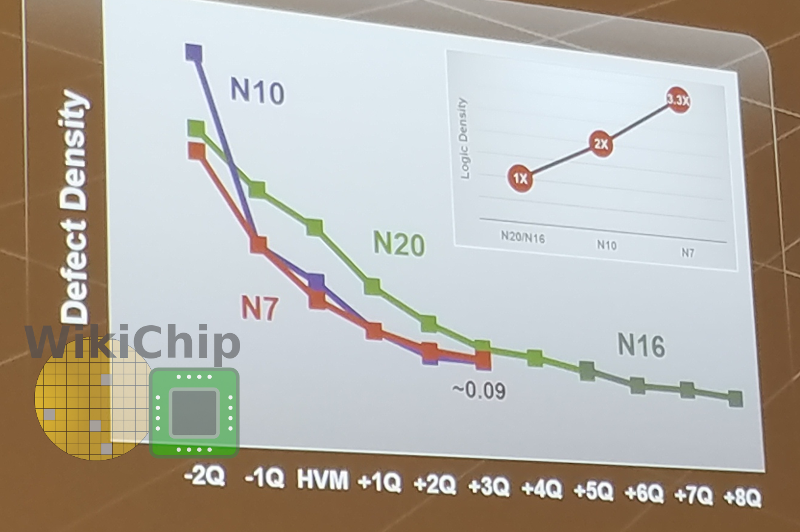
7nm is sitting at ~.09 defect rate. VERY good.

That translates into:

Navi 10: ~80% Yield of fully working parts.
Zen2 Chiplet: ~94% Yield of fully working parts.

For years I have been saying, they don't make lower core count parts because they need to recover bad dies, they make lower core count parts almost entirely out of fully working parts, for segmentation purposes. This should help illustrate that.

The slide:
tsmc-n16-7-yield.png
 
Samsung is making Ampere, not TSMC.

Remains to be seen:
https://pcper.com/2019/07/nvidia-working-with-both-samsung-and-tsmc-for-ampere/
... they commented on the rumors and speculation with this statement from Debora Shoquist, Executive VP of Operations: “Recent reports are incorrect – NVIDIA’s next-generation GPU will continue to be produced at TSMC. NVIDIA already uses both TSMC and Samsung for manufacturing, and we plan to use both foundries for our next-generation GPU products.”​
 
For years I have been saying, they don't make lower core count parts because they need to recover bad dies, they make lower core count parts almost entirely out of fully working parts, for segmentation purposes. This should help illustrate that.

Not likely that elegant of a "solution" to suggest it's all artificial fragmentation -- how they are reporting defects makes a difference. And with these dimensions, a yielded core will have variable performance, so there will be qualifications on that as well (e.g 2 dumpster fire, but working, cores out of 8 makes a great 6 core chip).

It's still great news. Now we need Intel to knock it out of the park as well because we want competition at the bleeding edge.

We aren't talking about "solutions". We are talking facts.

A defect rate is standard reporting mechanism for a process, it isn't dependent on disabling redundant parts. That's why it's actually better to have than yield number, which could arguably change depending on redundant parts, and definitely changes dependent on die size. Every once in a while Yield rates would slip out and they were typically in the 90% rate, but again that is the one subject to interpretation and size.

With the defect rate, you can calculate fully enabled parts yields of various sizes.

Sure there will be speed binning, but that is a different issue.

Through the history of silicon parts, the majority of disabled parts have been all about segmentation. Sure they enable some recover of partially defected die, but that is a bonus.
 
You're correct I flipped yield and defect density, my apologies. Although I haven't seen an official statement as to what TSMC is calling a defect; https://en.wikichip.org/wiki/defect_density leaves some ambiguity. A core disabling defect is different to a defect that renders an entire chip dead--I would imagine that they are using a more conservative number, i.e. any defect that renders a logic block dead (whether or not that chip can be saved).

For years I have been saying, they don't make lower core count parts because they need to recover bad dies, they make lower core count parts almost entirely out of fully working parts, for segmentation purposes. This should help illustrate that.

Simplistic ideas are "solutions" to a complex problem and low defect density does not quite so neatly translate into a segmentation strategy. Speed binning *is* a form of segmentation, which is why I said a zero killer defect 8-core chip with 2 weak cores will be sold as a 6 core part. Disabling hyperthreading on older parts enabled weaker cores to be up-rated in capability. Or cache blocks, etc. Unless we have a clear idea of the ATE suite of stress tests and the heuristics used on the back side of QC to separate out parts, it's difficult to back up your assertion, even if to the public eye it appears as you describe.
 
Simplistic ideas are "solutions" to a complex problem and low defect density does not quite so neatly translate into a segmentation strategy. Speed binning *is* a form of segmentation, which is why I said a zero killer defect 8-core chip with 2 weak cores will be sold as a 6 core part. Disabling hyperthreading on older parts enabled weaker cores to be up-rated in capability. Or cache blocks, etc. Unless we have a clear idea of the ATE suite of stress tests and the heuristics used on the back side of QC to separate out parts, it's difficult to back up your assertion, even if to the public eye it appears as you describe.


Segmentation would still happen if they had 100% perfect yield.

Disabling good parts is often done, even outside of silicon. I remember decades ago there were calculators where the less advanced models were exactly the same, fully populated circuit boards as the advanced models, but they just had some of the extra function buttons covered in the case.

People seem to have a hard time understanding that there is a place for disabling HW and selling it for less, though they don't have an issue when they do this for software.
 
Back
Top